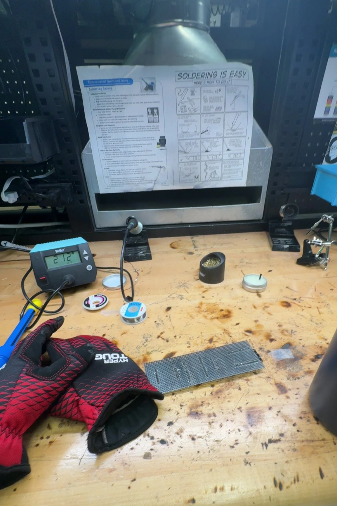
University of South Florida Multifunction Nanobio Materials and Composites Lab
I was lucky enough to work under the direct mentorship of David Oloruntobo and Dr. Ali Ashraf during May - August 2026. I learned tremendous amounts through the fast-paced environment. Projects needed to be completed and I would be placed on them as an Electrical Engineer Lead often times with little to no previous experience in the field.
This type of engagement allowed me to work in a team setting while simultaneously learning independently. Work was often required to be done on a tight budget allowing for even more engagement with the material to understand the most effective and cheap way to innovate.
Below are some highlights of what I worked during my time in the lab.
INSOLE CIRCUIT DESIGN
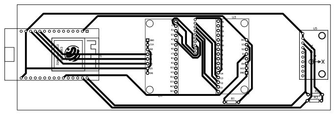
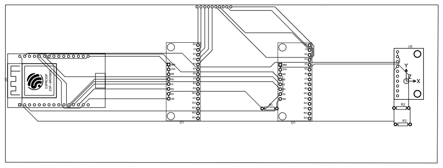
I designed this early layout of the circuitry of our insole.
Given constrictions such as the ESP32 needing to be on an edge, I had to accommodate the design accordingly. Another constriction as seen in the circuit design is that the circuit had to be one sided because of budget restrictions limiting us to manufacture the circuit in lab rather than offloading manufacturing to a factory.
After much trial and error the team reached this final design. It integrates the ESP32, 2 Multiplexers, and an accelerometer.
This circuit was then manufactured on a flexible PCB that wraps around the ankle, allowing proximity to the insole.